
During Summer 2014’s hedonistic highs. The vastly increased muscle mass, versatility and popularity of mobile computing devices led many authoritative and commanding sources to declare the desktop computer would soon occupy nothing more than a chapter in Grove’s dictionary of Silicone.
Smartphones provided the ability shoot and edit High Definition video. Tablet devices afforded their users both a rich gaming experience and remarkable desktop publishing potential while the trusty old Laptop, if assembled with the finest components, arguably offered graphical, data processing and transfer tempi comparable to that of cutting edge Towers of Power barely six months old.
Despite such prophetic proclamations and debatebly evident realities, the wheels on Intel’s wagon of thick cut “Desktop Dripping Chips” continued to rotate at a healthy velocity. Over the preceding half decade, we witnessed the release of an almost befuddling number of motherboard chipsets targeting any and all owners of a desk and more than a single square centimetre of real estate left to occupy.
A brief excursion into the archives of this site will reveal how this coincided with Intel’s assertive “socket designation policy” for every resulting customer. Moreover, as each chipset emerged, our venerable third party motherboard maestros repeatedly went into furious overdrive, introducing a maelstrom of supposedly “exciting” and ” practical” features in abundant excess of Intel’s call of duty.
Despite such tangible efforts to refine, there remained significant confusion, not only over which CPUs one could expect to be compatible with motherboards they had purchased but also which other key enhancements they had acquired that would further future proof their systems
The reason behind the influx of flummoxed forumers that the already established chip giant and rapidly evolving board behemoths (Asus being the largest), rarely met up for a pleasant spell of Sunday scheming, and when they did, seldom were any plans thoroughly perused and compared. Each was far more concerned over his own future status and perhaps about how it could cease to depend on another’s strategy. If none could grasp absolute power, they could at least have fun pretending.
In order to better understand when and why the waters were muddied, let us glance at a brief timeline documenting several of Intel’s designs, of how they were interpreted by their original composer, and some lavish paraphrases by his most prominent contemporary, Asus.
In order to preserve a little clarity, we shall only focus on chipsets aimed at the high end mainstream and enthusiast markets.
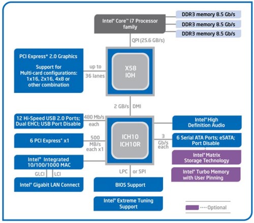
A chipset for the enthusiast and the first from intel to officially support SLI following Nvidia’s withdrawal from the motherboard market.
The new socket design 1366 was initially compatible with three new core i7 45nm chips, the i7 920, i7 940 and i7 965 “extreme edition”. All were quad core with hyper threading and based on Intel’s “Nehalem” architecture.
Other notable features included:
Now let’s take a look at the first boards Intel and Asus assembled to house these silicone saplings.
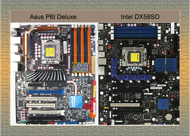
Enthusiast joe 1: Hmm. Ok, nice and simple so far…..uh….just a couple of things dear sirs. Mr. Asus I can’t help but notice your board has six memory slots and Mr. Intel, yours only has four, any reason?
Mr Intel: My bountiful blueprint makes things very clear, tri channel memory, a total of 25.6 gigabytes per second of bandwidth for the user, that is what I have provided.
Enthusiast joe 2: I see, Mr Asus, because your board has six, doesn’t that mean double the bandwidth.
Mr. Asus: No, bandwidth is exactly the same and its still three channels, but we thought it might be helpful to provide an extra three slots for those who want both tri channel and the maximum amount of memory Mr. Intel’s chipset allows for, more memory might not mean more actual bandwidth but it certainly helps speed up certain applications.
Enthusiast joe 1: Mr. Asus does have a point there, your chipset will permit a maximum of 24gb of memory
Mr Intel: As far as I am concerned I have implemented exactly what I promised, triple channel DDR3, nowhere do I state a maximum on my blueprints and if I had done it would have said “upto 24gb”, this is a limit that Mr. Asus has chosen to exploit and I’m sure his customers shall be most satisfied. Every key feature on both our boards is the same. The Same memory bandwidth, the same PCI Express speed, the same number of PCI Express lanes and so on.
Enthusiast joe 2: And both board support the same processors?
Mr Intel: Absolutely.
Mr. Asus: Quite correct
Enthusiast joe 1: Fair enough, I think I’ll take Your board Mr. Intel, its a little cheaper and having a board made by the manufacturer of the chipset sounds like a pretty safe bet, I’ll be using it with an i7 940 chip, I hope it’ll serve me well, .
Enthusiast joe 2: I’m going with Asus, could do with the extra memory and no doubt the over clocking facilities will be excellent. I’m breaking the bank with and i7 965 Extreme, just can’t resist having the best, hope its worth it!
———————————————————————————–
Not much more than a year passes, during which our micro machinating Megladon (that’s Intel) decides to unleash a clutch of new processors. These included the i7 930, i7 950, i7 960 and i7 975 Extreme. Each is again a quad core 45nm chip based on the same 1366 socket design and “Nehalem” architecture. The only variable is the speed and both of our average Joe’s were delighted to discover that each of their boards would be compatible with all 4 cpus by way of BIOS upgrades provided by their respective manufacturers.
Throughout 2010 and the first half of 2011, a further four new CPUs emerge, in terms of their external physical dimensions, these chips are exactly the same as their socket 1366 ancestors but this time, under their heat spreaders, a few noteworthy upgrades resided. First, a smaller die christened “Westmere”. Just 32nm instead of 45, consuming less energy, generating less heat, and paving the way for overclockers to achieve superior results. Second, an extra two cores, each with hyper threading, making 12 data crunching threads in total. Another tantalizing prospect for our enthusiastic Joes.
Once more, both Intel and Asus readily provided a bios to afford each the chance of a beneficial and convenient upgrade.
Z68 (May 2011)
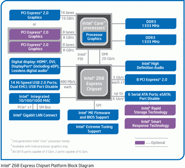
A chipset for the performance concious main-stream user. The z68 was Intel’s second such platform – following the p67 six months earlier – to support its 32nm “Sandy Bridge” generation of processors and thus represented a “refresh” of existing technology.
The z68 inherited the p67’s 1155 pin socket design which at the time, was compatible with no less than 14 CPUs. These were a combination of core i3, core i5 and core i7 chips with speeds upto 3.4ghz. Those in the core i3 family had two processing cores under the hood, the core i5’s boasted four and the core i7s also harboured four but with Hyperthreading active on each. Water’s a little muddier now?
Other notable features included:
Notable absences included:
Two sparkling boards lay in waiting…
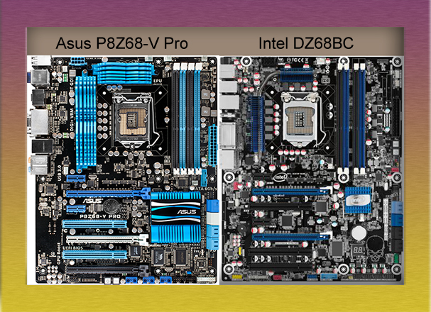
Average Joe 1: Hmm, ok, that’s a lot of processors to choose from….
Mr. Intel: Would you like a list sir?
Average Joe 1: Uh, yes please.
Mr Intel: Here you are…..
Average Joe 1: Rrrright….emmm….why do some have letters at the end even though they run at the same speed?
Mr. Intel: The K means the chip has an unlocked multiplier, previously only my “extreme edition” creations carried this feature, it allows for…..
Mr. Asus: Great overclocking, my board overclocks like you won’t believe, got more on the way aswell…..loads more…wait till you see the Maximus and the Gene…and the…
Mr. Intel: Thank you Mr. Asus, the S means a lower power chip. The 2600S for instance consumes 30 watts less than the 2600k, better for those of you desiring cool, efficient and silent systems.
Average Joe 2: Is there any reason you didn’t combine these features so we could have the best of both worlds, would be a been a little less confusing too.
Mr. Intel: I needn’t have provided either….and I believe choice to be a very healthy thing.
Average Joe 1: OK. Well, I’m taking the Asus, always have and probably always will, along with a 2500K, should be well upto any task I throw at it, plus more than a spot of gaming!
Average Joe 2: I’m going for Intel this time, can’t see too much difference and I’ll take it with a 2400, just want something stable, fast and future proof.
Mr. Asus and Mr. Intel are silent.
Our Average Joes are content with their purchases, but as 2012 dawned, each learned of a new standard of PCI Express, revision 3.0, which was to offer double the bandwidth of the present version and be readily adopted by, amongst others, our two old friends at green and red HQ, Nvidia and AMD in their eternal struggle for graphical glory. With both Joe’s planning to upgrade their video cards, they wondered if their motherboard’s would be able to fully exploit the potential of this coming and future generations.
Average Joe 2: Uh, Mr Intel, I just wanted to know I my motherboard will allow me to take full advantage of the new pci express 3.0 graphics cards Nvidia’s planning next year.
Mr Intel: My chipset’s specification is very clear 16 pci express lanes configurable as either 1 slot running at x16 or two running at 8, all revision 2.0.
Average Joe 2: oh, so no chance of a bios update to enable support for pci express 3.0.
Mr Intel: I state nothing that is not in my official specifications, though such support wouldn’t be possible with a BIOS update. Future PCI-E 3.0 cards will in theory function in your board since the standard is backwardly compatible but they will only run at the speed PCI-E 2.0 allows. I’ll be offering full PCI-E 3.0 support with my next sensational chipset and miraculous “Ivy Bridge” processors, which I refuse to talk about right now.
Average Joe 1: Mr Asus? I have just purchased this, it’s AMD’s new Radeon HD 7970, a PCI-Express 3.0 video card, will it run to it’s full potential in the board I acquired from you, that’s the P8-Z68-V Pro?
Mr Asus: No it won’t, in order to obtain full PCI-E 3.0 support you’ll need one of our “GEN 3”, like this one:
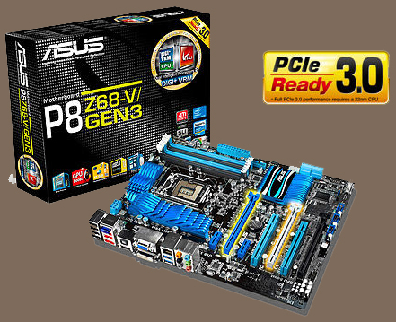
Average Joe 1: But that’s the board I have, at least, it looks identical.
Mr Asus: Not quite, see right there, above the first PCI-Express slot, those little chips are bridge chips known as “switching ICs”, they sit in between the CPU and your PCI Express slots and are required when you run multiple video cards, to allocate equal bandwidth to each. When I built your board, the only switches that were available supported PCI-Express 2.0, these new ones came out a few months later.
Average Joe 1: Really? So, any reason you didn’t wait and just release this one, wouldn’t it have been less confusing.
Mr Asus: Intel releases a chipset, I’m compelled to forge accompanying boards immediately, its what I do, I have many rivals doing the same, look at what Asrock and Gigabyte are upto these days. I have lots of other GEN 3 boards now if you’d like to see them.
Average Joe 1: No that’s ok, I’ll be off now.
Average Joe 2: Excuse me Mr Asus, I spoke to Mr. Intel about this and he said he’d only be supporting PCI Express 3.0 on his next chipset.
Mr. Asus: That’s sort of corrent, For PCI Express 3.0 to actually work, you will need one of his new “Ivy Bridge” CPU’s as well, the controller in the “Sandy Bridge” processors only supports 2.0. But look, you don’t have to wait for his chipset or any boards he might knock up, why not just get one of my Gen 3 boards now and be fully prepared for when the processors arrive, then if the chipset turns out to be a real hit, come back and buy another of my boards and transfer the processor over to that. Wait till you see the line up I have planned. There’s a workstation series, a P8 series, should please you that one, my Republic of Gamers line, the Sabretooth….ohhh I can’t wait.
A few months later, in April, our silicone sorcerer true to his word, conjured up another new chipset…
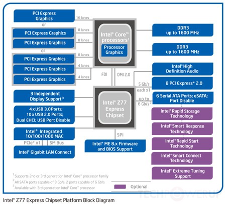
The third in little over a year to incorporate the same 1155 pin socket. Moreover, a novel brigade of processors materialise alongside it. Once again, externally they and their elders were physical dead ringers, though just as the “Westmere” had been the “Nehalem’s”” refined successor, so too were these chips destined to displace clan “Sandy Bridge”. Beneath each heat spreader resided over a billion of Intel’s revolutionary tri gate 3d transistors packed into four cores on a smaller die of 22nm, all representing a 20% reduction in energy consumption and a performance increase to match.
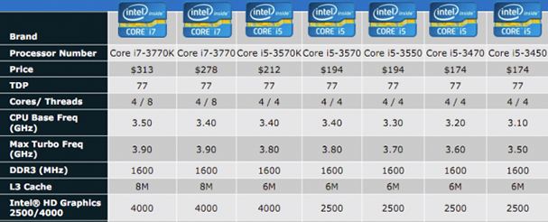
A markedly fleeter and more versatile integrated graphics chip was also present along with 4 native USB 3.0 ports. Improvements had been made to “Quick Sync”, a feature introduced in the Sandy Bridge era to greatly reduce video rendering and decoding times, DDR3 speeds of upto 1600mhz were officially supported and finally, as pledged, the Ivy Bridge’s built in PCI Express controller served up 16 lanes of third generation bandwidth bandwidth to any designated slot.
Our average Joes, perhaps a little blitzed in the brain as well as the pockets, do not wish to undergo the inconveniences of a full system overhaul. With both their builds proving stable and efficient, the option of enduring this minor setback seemed far more attractive. PCI Express 2.0 should surely be fast enough for now. All the same. The benefits the new Ivy Bridge CPUs appear to offer are tempting, the question was, were they compatible with the boards they had already invested in?
To their great relief, both Intel and Asus promptly compiled a BIOS update to allow Joe 1, Joe 2 and others whose motherboards harboured Intel’s earlier chipsets, the opportunity to revel in the enhancements an”Ivy Bridge” CPU granted….excluding PCI Express 3.0!
Z87 (May 2013)
Fast forward another year and our tyrant of transistors is at it again.
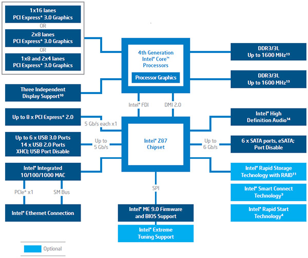
The z87 was another chipset aimed at the mainstream user who craved the best possible performance from a decent but ultimately sensible budget. As the z77’s successor, it also proved to be the vessel that carried us into Intel’s fourth generation of “Core” based architecture and gave birth to the the “Haswell” family. These processors occupied a new socket lined with 1150 pins and were twelve in number at launch. Each, like their predecessors contained four cores on a 22nm die with Intel proudly proclaiming performance increases of upto 15% in frequent scenarios. Base speeds ranged upto 3.5ghz and turbo frequencies, a maximum of 3.9ghz. The family consisted of six core i5 chips and six core i7 and in keeping the the “Sandy Bridge” tradition, only the core i7s possessed the ability to hyperthread their way through data.
Other notable features included:
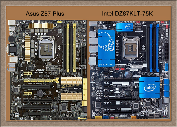
Fresh from production and still emitting the delicate fragrance of lacquer, two more magnificent maternal essentials were eager to serve.
Another Average Joe 1: Ok, Mr Intel, so 12 CPUs this time?
Mr Intel: Not quite, one of them, the Core i7-4770R , is in integrated model I intend for manufacturers to weave directly into their circuitry, you’ll have to wait a while for those, here’s the full menu.
Mr Intel: Remember, it’s K for an unlocked multiplier, S for lower energy consumption, oh yes and I’ve added a third, T, extremely low energy consumption, 20 watts less again to be exact…
Mr Asus: Wait till you see the features of my board. My new software, AISuite three has four way optimization which can over clock your CPU automatically by applying a series of fantastically accurate incremental stress tests. You can configure it for raw performance or maximum economy in just a few clicks. I have an alternative to that board too, well several actually, there’s my Z87-K, Z87-C, Z87-A Z87M-Plus, Z87 Pro, Z87 Expert, Z87-Deluxe, Z87 Deluxe Dual and Z87 Deluxe Quad, some have Wifi and thunderbolt connectors instead of the extra video outputs…and Sata Express ports, have you heard about that, for drives even faster than Sata 3.0, I’ll be offering those too…
Another Average Joe 2: WOOOOOHAAAA, that’s NINE motherboards, all based on the same chipset.
Mr Intel: I guess that’s what happens when you are less strict with your guidelines, no matter!
Mr Asus: No, there’s the Z87-WS too and the Sabretooth Z87, and I have five Republic of Gamers boards in the pipeline, let me tell you….
Another Average Joe 2: No no no no, you can stop right there this z87 plus will do fine just fine and I’ll take a 4770K with it please, can’t wait to clock it to Hades!
Another Average Joe 1: Well, sometimes choices can be too agonizing, I’ll go with your board Mr. Intel, has a few less SATA ports but a couple more PCI Express slots, I have quite a few peripheral cards so those will be useful, and I’ll take a 4770T to boot.
——————————————————————————————————
As 2013 ran its course, our other average joes benefited greatly from their acquisitions as much gaming, video editing, surfing, music making, skyping and plain old fashioned hard work ensued.
The first half of 2014 saw Mr Asus continue to vigorously harvest PCBs and forge board after board while Mr Intel attended to his corporate clients and their insatiable lust for Xeons (let’s not go there…this is really getting tiring). It wasn’t until early summer that our supreme master of the cores (that’s Intel) found himself in dire need of some main stream refreshments…and for our average Joes, this is where the story really starts.
Z97 (May 2014)
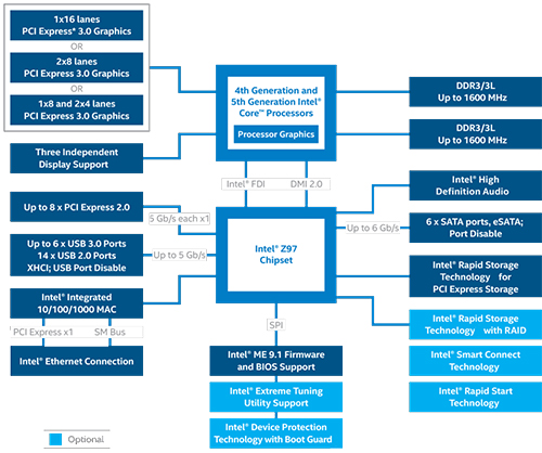
The z97 was, as the z68 had been, a refinement and enhancement of existing technology though this time, barely anything appeared to distinguish it from what it was to supplant. There was official support for the M.2, an interface compatible with the imminent generation of mobile SSDs, but very little, if anything else.
Another Average Joe 1: Mr Intel I couldn’t help noticing this new chipset of yours, it seems so very similar to the last, what possible reason could you have for bestowing it upon us.
Mr Intel: What use would my resplendent assemblage of fresh CPUs be without am elegant chipset to accompany them?
Another Average Joe 1: More new processors?
Mr Intel: Of course, known as the Devil’s Canyon two stunning quad core Haswell thoroughbreds, each with unlocked multipliers, a fresh coat of polymer thermal interface on top, a sprinkling of extra capacitors underneath. The i7 4790k is undoubtedly a marvel, one of my finest ever, a base frequency of 4ghz!
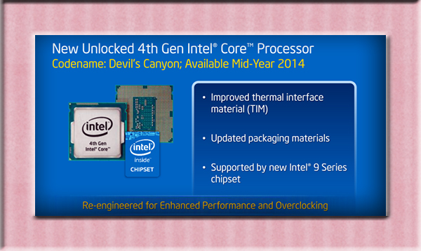
Another Average Joe 1: The same socket as before.
Mr Intel: Absolutely.
Another Average Joe 1: So I could go and upgrade right now, just drop it into the your board, remember the one? The DZ87-KLT or will I need a BIOS update.
Mr Intel: No…I won’t be providing a BIOS update, these processors will not be officially supported by your board. I’m afraid my motherboard days are over and I intend to apply my genius solely to other imminent chipset and prolific processor projects aswell as various completely original and indispensable creations I’ll divulge when the time is right. Goodbye.
Another Average Joe 2: Excuse me, Mr Asus, I’ve just heard about these new Processor’s….
Mr. Asus: The Devil’s canyons?
Another Average Joe 2: YES, that’s right.
Mr Asus: Don’t worry, we have a BIOS update in hand and ready for downloading.
Another Average Joe 2: Oh, fantastic, I was afraid I would have to shell out for one of your z97 boards, I assume you have plenty.
Mr Asus: Indeed and I should imagine your friend will be shelling out for one before too long. Mr Intel. He should have stuck to chipsets from the outset, one less rival to fret over, motherboard mastery, that’s always been my game.
——————————————————————–
The sad and cruel truth is that this was not the first time Mr. Intel had neglected the loyal customer. Complacency, careless oversights and misleading marketing techniques were also palpable amidst his Enthusiasts, where the x58 chipset had began our story on such a positive note. It’s “Sandy Bridge” successor, the x79 had emerged from the den of dies at the end of 2011 with its own duo of 6 core “Sandy Bridge-Extreme” purse pilferers – to which a further two were added the following year – and whilst initially boasting notable advantages over its mainstream counterpart (40 PCI Express lanes, and quad channel memory being the most seductive), it was Intel’s main stream users that were granted two new chipsets (the z77 and Z87) in addition to the chance of acquiring “Ivy Bridge” and “Haswell” architecture before the x79 was given a second glance.
Moreover, the confusion regarding PCI Express 3.0 that had so vexed our average Joes was again manifest, with Mr. Intel boldy asserting his chipset and processors faithfully delivered a double helping of bandwidth to any multi GPU configuration but old Giant Green Eyes (that’s nvidia) refusing to guarantee his brand new video cards would utilize it due to a “variation in signal timing generated by your chipset and processors”. A patch was subsequently handed out for customers to apply at their own risk.
The second glance referred to above, was to eventually bring forth a trio of “Ivy Bridge Extreme” processors but no complementary chipset refresh and in falling so far behind the mainstream product line’s pace, these enthusiast class CPUs appeared adopt the “Haswell” naming convention, perhaps leading to some suggestions of misleading advertising. The final noteworthy negative was Mr. Intel’s prompt and all too familiar dissertation of its very own renditions, the DX79SI and DX79SR, both flagship motherboards aggressively aimed at our eager enthusiasts, would now never be officially compatible with these new CPUs.
To any and all reading this, I attempt to remain in the past tense for good reason, it saves money and preserves relevance. The next one will be shorter! X99 anyone?