The Case of the Befuddling Base Clock
One frosty eve in the Winter of the foremost annul of the millennium’s second decade, a weeping, westerly sun lay low its rueful rays and retreated beneath a cumulus curtain, one that cloaked the Earth’s stage and solemnly marked a chip-set’s final hour in office. Over one thousand days of legendary service in stoic honour of gruelling gaming, onerous over clocking , fathomless folding, remorseless rendering, preposterous priming and murderous mining….have I used any of those before? I am of coarse waxing lyrical over the virtues of the x58. Pin for Pin and cap for cap, Master Intel’s most versatile, least volatile and luxury laden answer to an enthusiast’s uncompromising aspirations.
When married to its accompanying processors, the Nehalem derived “Bloomfield” and later, the “Westmere based “Gulftown”, this noble flagship ferried a small fraternity of allegedly favourable innovations.
First and foremost, a relocated memory controller, dragged from its classy North Bridge abode and dropped into small apartment under the processor’s heat spreader.
Next up. The Uncore. Not a tangible feature, but the expression used somewhat ambiguously, to collectively define components critical to the CPU’s functionality but not resident on its core(s). Precisely what the term accounted for varied from one platform to the next and occasionally encompassed elements of the motherboard. Inevitably, it depended on the views of experts who sought pleasure through perpetual disagreement and obfuscation. Thankfully, I’m no such expert, but for the purposes of this article, feel free to consider the Level 3 cache and memory controller as two primary examples of what the Uncore represented.
Third in line was the QPI, or Quick path Interconnect. A bountifully broad bi-directional data conveyor, effortlessly encapsulating and efficiently transporting the system’s cumulative binary payload from the processor’s cores to the IOH, formerly the North Bridge, and returning it in a more timely fashion than a cheetah’s application for a job at an institute for suicidal antelopes.
Each of the above was attributed to an independent multiplier which, for the Uncore, had to be at least double or one and a half times that of the memory, depending on whether a Bloomfield or Gulftown CPU was installed, while all three were inextricably bound to a fourth and definitive catalyst, the beguilingly “flexible” base clock.
This proverbial “magic bullet” was the divisor, factor or increment which ultimately dictated the frequency of the CPU, QPI, Uncore and RAM by virtue of their respective multipliers. The value was decreed by Intel and resided at 133mhz in the case of every Nehalem and Westmere variant.
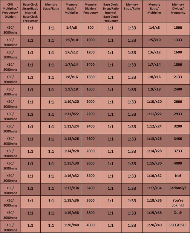
With the aim to better comprehend this steady accumulation of digits and descriptors, here is a delicate dusting of appropriate visual assistance.

As you can observe, the multipliers equate to ratios which can be interpreted in the same fashion as basic betting odds. The lower figure denotes the better’s stake and the higher, the bookmaker’s return in the event of a triumph. To apply the analogy, think of the processor’s “stake” as whatever its base clock divisor is, in this instance, 133mhz. Then times that figure by the value of its multiplier to get the CPU’s “winning” frequency!
The same logic can be employed to ascertain the speeds of the QPI, Uncore and Memory since all are comprised of the base clock’s numerical building blocks.
In regard to these arbitrarily animated aids, which hopefully will emanate quaint and enlightening quirkiness amidst a storm of supercilious synonyms, the frequency ranges quoted for the processor and memory are based on the advertised specifications of all compatible parts. They do not account for the additional performance one might achieve by skilfully exploiting several billion BIOS specifics. Consolidating this data would be impossible since every motherboard embodies different options for fine adjustments, which generate uniquely contrasting increases in speed.
For processors, the values relate to the slowest chip in a non-turbo state, to the fastest with turbo enabled. In this case, the applicable CPUs are the Bloomfield i7 920 and i7 Gulftown 990 Extreme Edition respectively. Regarding RAM, the figures listed coincide with the vendor’s certifications for kits with the lowest and highest bandwidth. Though never much in demand, introductory DDR3 modules commenced at frequencies of 800mhz with supercharged sticks stretching to 3000mhz once fabrication techniques had reached their zenith.
Here are some important equations to commit to your cortex before we proceed.
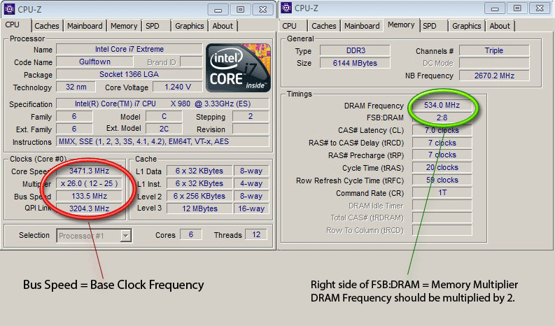
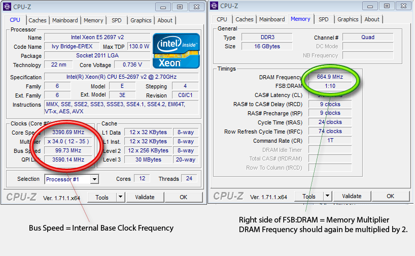
Memory Multiplier = Right side of ratio (DRAM:FSB) as listed in under the memory tab of CPU-Z.
Memory Ratio = The above figure divided by 2.
Memory Frequency = Base Clock x Memory Multiplier
QPI Frequency = Base Clock x QPI Ratio/Multiplier
Uncore Frequency = Base Clock x Uncore Multiplier
DDR SDRAM = Double Data Rate Synchronous Dynamic Random Access Memory, with a clear emphasis on double.
The RAM frequency CPU-Z displays amounts to half of its actual value, while the identified memory ratio is double what it should be. Put simply, the first figure accounts for the memory’s disposition to duplicate, while the second does not? Why? Because its so delightfully confusing. Just bare in mind, when incorporating the memory’s ratio to calculate its speed, you’ll need to double up to get an accurate result!
Alternatively, to avoid your lobes spontaneously liquidizing and elude a succession of superfluous clicks, you could defiantly discount the ratio and work solely off the readings that CPU-Z delivers, praying that purists don’t descend upon for you doing things the easy way.
Our Story Moves On
As speculation concerning the potential of what had promised to be a momentous architectural transition gathered steam, thoughts amongst the tuner’s elite were initially mixed. The long standing Front Side Bus had proven a pivotal variable on which all hampered by fixed multipliers relied, and its removal apparently relegated the motherboard’s role in scaling mount megahertz to one of meagre significance.
For those who were looking to preclude profligacy but procure perks by avoiding Intel’s extortionate extremists, this was declared an imminent disaster. Oh! Horror. Frequency would be founded on fabrication alone, an arbitrary asset determined by acquiring a processor whose cores were its maternal wafer’s crisp and crunchy prime cuts, or charred and chewy cold cuts.
Obsessive over-clocking omnipotence was over. The motherboard was but a shell shorn of all senses, a silicone slave, perpetually perturbed by her pilot’s proclivities. The Bloomfield’s burdensome base clock would sneakily scupper any sizeable speed bonus while the diminished on-die memory controller and QPI were rumoured to harbour multipliers locked tighter than Bluebeard’s briefcase. Worse yet, what would become of RAM when compromised by its crippled custodian, whose competence to safely supply sustenance subsided at 1.65 volts? Oh! Havoc! Venture above this, and your ship would flounder in flames, before sinking below bilious blue smoke. By the damnation of SIMMS, were the days of deluxe DIMMS also dwindling to a close?
Thankfully, the universes’s greatest healer was at hand. Time. Soon, such portentous prophecies would be exposed as pre-emptive paranoia originating from adopters who might well have camped beside factory lines. The immobilized QPI and memory multiplier were inhibitions subsequently associated with non-retail CPUs, otherwise known as “engineering samples”.
The merciless martinet Intel and his ceaselessly shrewd opportunism, had already spawned a second welcome remedy for the DDR dilemma in the shape of XMP (extreme memory profile). This was a convenience identical in concept and function to SPD (serial presence detect), collaboratively developed by Intel and “accredited” memory vendors. It allowed for a modules’ most important settings pertaining to timing, frequency and voltage to to be stored in a small chip on the stick (the EEProm) then activated in the host motherboard’s BIOS via a single keystroke, and with the manufacturer’s formal approval.
Packages typically presented a pair of intuitive “profiles” influenced by probable real world scenarios, some with taut, “aggressive” timings and command rates at the price of frequency and others with loose “relaxed” timings and higher frequencies to maximize bandwidth. Now is not the moment to discuss or debate the merits of either so I shall suitably simplify “tight and low” for game nation “loose and high” for creation. Bah! Unfit to trammel a hip-hoppers trouser sag. To further placate the panic, memory vendors themselves were in radical form and, like Japanese motor machinists extracting voluminous velocity from humble handfuls of horse power, utilized 1.65 volts to work modular miracles.
Masterful motherboard innovators imbued with instincts to circumnavigate and conquer coded rebellious BIOSES replete with screen after screen of scalable voltages, memory timing and latency tweaks.
By 2014, many initial doubters, some fonts of knowledge on popular podcasts probing cutting edge technology, were stubbornly shunning all Haswell wholesomeness in favour of their six year old i7-920, out of which they had cranked a shade south of 5ghz from an officially authorized 2.66. Meanwhile, there were others that had parted with pounds to secure “extremes” (the i7-965) , all of whom were engaged in an quintessential quintet of over clocking splendour, with the RAM , CPU, QPI, Base clock and Uncore multipliers agreeably divorced and awarded absolute autonomy.
The forging of Sandybridge in 2011 brought forth another Intel bait and switch special. The privilege of adjustable multipliers to main stream processors at the expense of a base clock tightly tethered to every bus in the chipset. The PCIe, USB, and SATA controllers had converged into a military parade behind the memory and CPU. Nudge the “base” drum one hurt too high and reduce the regiment into cacophony of brassy dissonance. Liberated processors were distinguished by a “K” at the end of their call-sign and artfully targeted at those with even the tiniest tendency to tamper.
Extravagant enthusiasts crossing the same bridge by “Extreme” express a year later, once again faired slightly better.
The introduction of ratios, also called “straps”, effectively created a”phantom” base clock linked solely to the CPU and enabled two elevated, “virtual” tuning thresholds that were transparent to the preposterously petulant peripheral buses, all of which remained supervised by the actual system clock .
Ah! Hold hard a moment. Barely parsecs ago there was just the base clock. Now we’ve got a phantom base clock and a “system clock”. Is this crude technocracy, or extraordinary attention to narrative variation with a yearning to evoke captivating suspense?
I know. Frustrating isn’t it? Technology’s most glorified gurus garner grand gratification from attributing names to things that either don’t exist or already have more names than an identity thief with dissociative identity disorder. Nevertheless, I’m afraid what was previously the “base clock” has evolved into asymmetrical twins and the consequences of expounding on the mechanics of two “base clocks” are sure to induce repugnant confusion. Therefore, to sustain clarity in our journey through the oncoming paragraphs, some revised definitions are imperative.
Base Clock 1: – This will be referred to as the “base clock” and randomly preceded by the word “internal” so as to emphasise its exclusivity to the CPU and isolation from external encumbrances. Picture it in the same way as you would closed circuit television, in the sense that its signal is not broadcast to the outside world or in the current context, the CPU’s hypersensitive surroundings!
Base Clock 2: This shall be called the “system clock” or “host clock ” and should be considered the “true” base clock. It is what remained visible to the rest of the motherboard along with its fleet of finicky buses.
Fear not, following a assortment of statistically fortified tables, your mind will be ineffably enriched. But for now, its…
Back to the Straps
Why, you may ask, was such a function devised? It would certainly have been useful for those impeded by imprisoned multipliers, but in staunch keeping with tradition, Intel had ensured that every shackled processor was also strapless and since unbound CPUs already offered comprehensive governance over their multipliers, where was the benefit in employing the base clock for more its bare essentials?
To paraphrase a cliché borne from journalisms tireless obsession with the negative , any granularity is good granularity.
Historically, processors of every age and pedigree have manifested richly varied patterns of behaviour when persuaded to violate their indigenous directives. Quite simply, they were complex creatures and for all who aspired to garner gigahertz, copious catalysts to customize generally delivered more positive returns than a BIOS whose menu’s were a wash of greyed out simplicity. One of the rules assiduously applied by specialists of many a generation, whether they be cranking the core or raising the RAM, was to keep every modification besides those necessary to nominate the desired frequencies as minuscule as possible.
In the case of Messrs Sandy and Ivy Bridge of non E descent, their cores were committed to scale in steps of 100mhz in accordance with their multipliers. A value of “x12” yielded 1200mhz (12 x 100) and one of x24 would give 2400mhz (24 x 100).
For fully audited members of the extremists’s lodge, these supplementary straps of 1.25 and 1.66 – some called them gears – allowed for previously untenable “effective” base clock speeds of 125 and 166 mhz to serve as raised starting points in addition to the 100mhz default. In other words, the CPU’s multiplier theoretically possessed markedly greater manoeuvrability and users could meticulously manipulate the cores’ frequencies over three separate ranges of approximately 15%.
It wasn’t until mid 2013 and the début of the intensely hyped Haswell the Intel saw fit to furnish his flourishing main-stream fraternity with the same delights.
The Haswell-E platform was intrinsically no different, and by this time, venerable motherboard moulders were vastly more enterprising, ambitious and perceptive, with many proficiently re-packaging the facility as an attractive USP.
The imperious, octo-dexterous 5960x – Haswell-E’s holiest – was stated by numerous impartial reviews to have obtained speeds approaching an impressive 4.5ghz . Promptly following its release and a brief spell under the fingers of feverish fiddlers, these claims were unanimously regarded as genuine. Such a pronounced injection of unconditional pace might have hovered beyond reach were it not for the base clock’s higher reference levels being successful in retaining a degree of unity.
The sole and risky option would have been to set the multiplier to x45, leave the host clock chugging along at 100mhz (45×100=4500mhz) and prey that no unpleasant bolts from the blue conspired to plague the poor ham strung user for imposing settings that strayed so far from stock.
However, in ascending to the middle strap of 1.25, hence triggering an internal base clock rate of 125mhz, this same tenacious technophile could decrease the multiplier to x36 (36×125=4500mhz), thereby ensuring closer alignment with its factory obligation but at negligible expense to speed.
The second and more pressing problem partially alleviated by our metronomic mediator concerned the accelerating evolution of memory. As new standards of RAM were conceived and commercialized, they were accompanied by a selection of independently approved and universally compatible defaults, ostensibly to avoid misunderstandings between manufacturers, whole-sellers, consumers and any other indispensable elements in the retail process.
The organization enlisted to formalize these vital guidelines was J.E.D.E.C. established in 1958 and actively engaged in similar roles throughout the electronics industry ever since.
J.E.D.E.C. ‘s draconian deliberations eventually divulged official recommendations for voltage, bandwidth and latency and were a conservative precursor to the aforementioned XMP profiles, formulated by Intel and pioneering memory vendors. Once formally ratified, they were indelibly written to the SPD Roms on the relevant parts during OEM production. Thereafter, it was up to illustrious brands such as Corsair, G.Skill, Patriot and others, to liaise with Intel and embrace direct responsibility for any optimistic deviations.
Did this deter their confidence? Not for a nano. Those Devilish DIMM die-hards abandoned convention more readily than a graffiti artist in the Pope’s bathroom and hastily unleashed their mightiest modules. According to Jedec, the maximum enforceable frequency for a juicy stick of DDR4 to yield a respectable combination of durability and fleetness was 2133mhz, exactly the same as they had endorsed for the final incarnation of DDR3.
In the initial period of DRAM’S fourth tenure, Corsair’s stunning stall consisted of several packages. Their revered “Dominator” lineage had sprouted a premium “Platinum” off shoot, which the company continued to cultivate with considerable conviction.
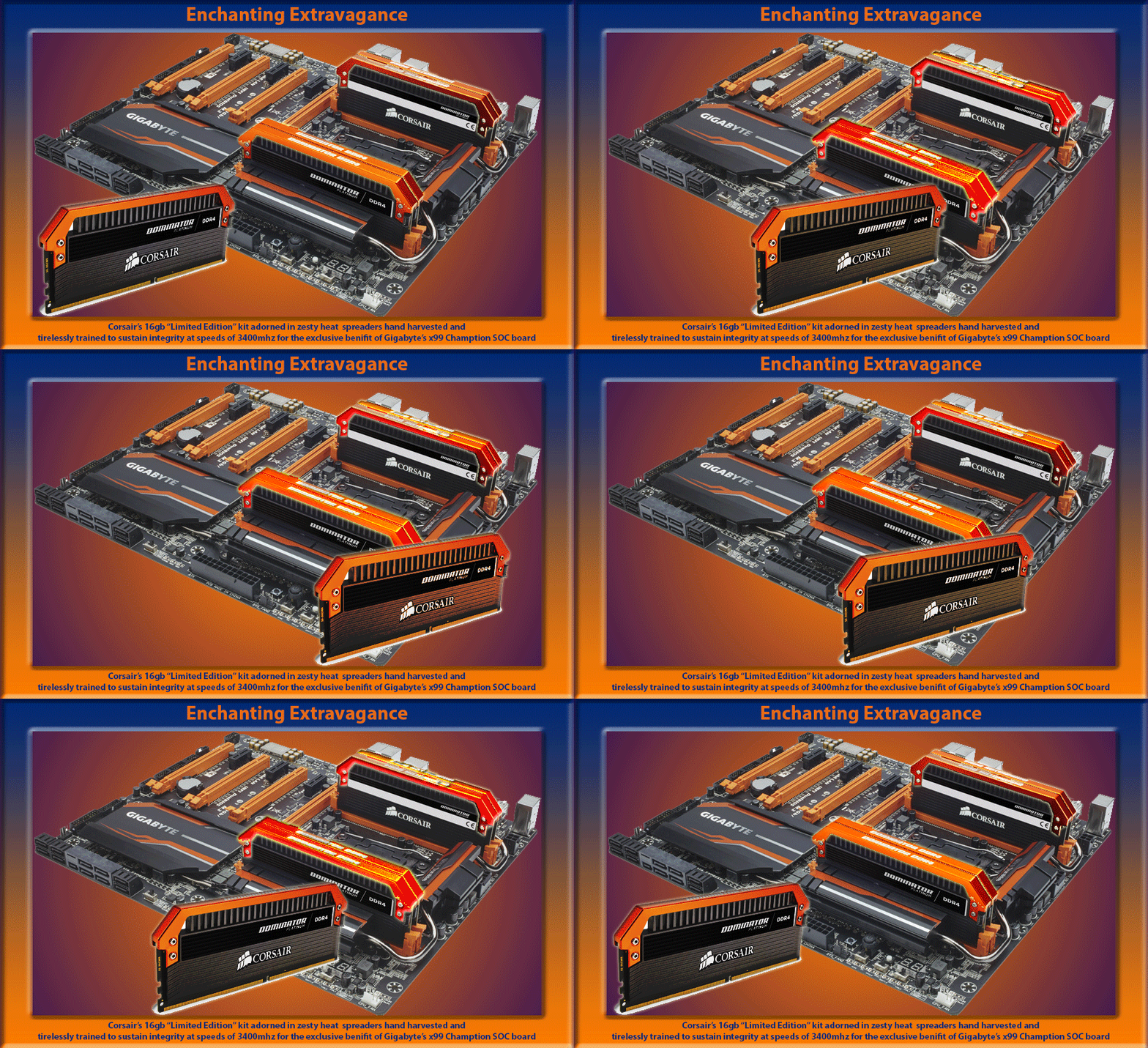
Advertised speeds ranged from at 2400mhz, already well in excess of JEDEC’s declarations, right up to an unprecedented 3400mhz for an limited set of four by fours arrayed in scintillating heat-spreaders of cinnamon-orange and reportedly verified to operate at their rated optimum by Corsair themselves. A rusty piece of DIMM and distant history for a peachy “Grand Mariner”, see what did there? Obscure allusions to the colour “orange”? Well, what better to stir up memories than memory itself?
To expend the bandwidth bestowed by class leading instruments of dynamic random recall should have been a motivating mission. However, as soon as one pondered the compulsory methodology and conceivable ramifications in attending to it, inspiration was abruptly overhauled by apprehension. Remember, the memory controller now shared room and board with the core(s) and any alterations made to the host clock would have a proportional and simultaneous influence upon the speeds of both.
Their statistical correlation was governed by the ratio separating the internal base clock and the memory controller. Depending on the RAM installed and value proposed for processor’s base clock, this ratio would affect an incremental ladder of frequencies for the memory, also known as “dividers”. For mainstream adopters of Sandy and Ivy Bridge based builds, these dividers were a bothersome impedance.
Though the resulting memory frequencies could be manually specified, the actual number available and their proximity to each other, lay at the mercy of Intel’s microcode and the intricacies of the motherboard’s BIOS. There was no certainty of a step on the ladder that would enable both the processor and memory to be close enough to their target frequencies to ensure stable or swifter operation.
Moreover, for the standard 100mhz host clock, even when factoring in its meagre flexibility, DRAM frequencies exceeding approximately 2666mhz were strictly out of bounds since memory frequencies climbed in steps of 266mhz and the steepest supported base clock to memory ratio was 1:10. (10X266 = 2666)
To partially assist, yet another strap situated between the base clock and memory ratio was introduced on the Ivy Bridge platform.
This strap, which for the sake of succinctness we’ll call the “memory strap”, imposed a ratio of either 1:1 or 1:33 relative to the CPU’s Base Clock. Thus, 1mhz for the base clock could represent 1 or 1.33mhz for the RAM and 100mhz translated to either the same, or 133mhz. In contrast to the Base Clock’s straps, neither memory strap offered any margin for fine tuning but its marriage to the existing memory ratios (or multiplier), meant that tweakers could now access two sets of frequencies (or dividers), one ascending in increments of 266mhz as before and the other in shallower steps of 200mhz. All of which made the puzzle of coaxing elite class DIMMS to comply with their prescribed and heavily publicised XMPs decidedly less daunting, and more likely to be solved at no cost to stability.
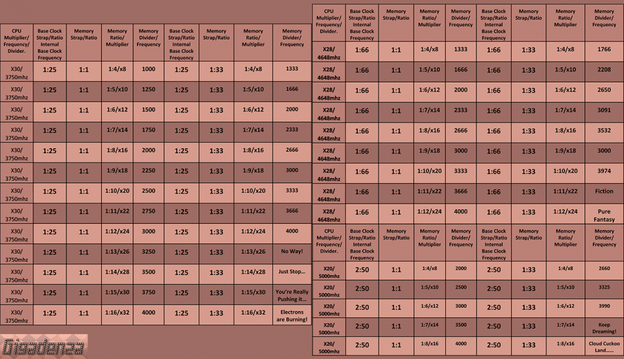
The Haswell and Hawell-E along with their accompanying chip sets, elegantly blended the bouncing base clock with the memory strap the to complement their investors with an exponentially augmented abundance of steps, straps, ratios, dividers and frequencies . Yes? And? How precisely does that cure our plight? A written response would involve too many figures to coherently construct in paragraphs, so let us proceed to absorb information in as pleasurable fashion as printed statistics will permit.

May I humbly present an inspiring, enlightening and indisputably imperative table (coming soon), artistically preceded by a graphical thesaurus (above) and a couple of complementary clipboard snippets (below).
Newly Applicable Formulae
CPU Frequency = Internal Base Clock frequency x CPU multiplier
CPU Frequency = Base Clock Ratio (Strap) x External System Clock Frequency x CPU multiplier (some people did it this way I have no idea which is more accurate or why and I’m extremely angry about that).
External System Clock Frequency = Internal Base Clock frequency / Base Clock Ratio (Strap)
Memory Frequency (if 1:33 memory strap/ratio used). Either can be used.
A:) 1.33 x Internal Base Clock Frequency x Memory ratio x 2
B:) 1.33 x Internal Base Clock Frequency x Memory Multiplier (as listed in CPU-Z)
C:) Base Clock Ratio x 1.33 x System Clock Frequency x Memory ratio x 2
D:) Base Clock Ratio x 1.33 x System Clock Frequency x Memory Multiplier (as listed in CPU-Z)
Memory Frequency (if 1:1 memory strap/ratio used). Either can be used.
A:) Internal Base Clock Frequency x Memory ratio x 2
B:) Internal Base Clock Frequency x Memory Multiplier (as listed in CPU-Z)
C:) Base Clock Ratio x System Clock Frequency x Memory ratio x 2
D:) Base Clock Ratio x System Clock Frequency x Memory Multiplier (as listed in CPU-Z)
For each group of memory calculations, solutions A and B are the most straightforward, though I was compelled to include C and D due to O.C.D brought on by the discovery of one solitary analysis that happened to favour them. Discount at your discretion. Manufacturers are notoriously inconsistent when it comes to selecting which parameters their BIOSES will incorporate and how they shall be expressed. I can only surmise the tweakers in question elected to rely on the figure their board declared for the systems clock and not multiply it by the base clock ratio, which would have given us the internal base clock frequency. Whatever the reason, the results are identical.
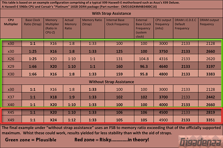
All figures in this table assume an absence of any plausible hindrance and are intended to illustrate the theoretical advantage of additional clock straps. They should not be interpreted as usable or even mildly competent advice!
Furthermore, due to motherboards affording broadly varied granularity, the values disclosed in the memory multiplier column should be considered hypothetical and will not necessarily reflect the choices your BIOS provides.
The uppermost spectrum commencing at a blazing base clock rate of 250mhz, was widely regarded as unenforceable at the instant these letters entered the ether, and two years earlier, it had been Asus who were suspiciously brisk to assert that no processor destined to permeate their laudably lavish laboratories was or would be capable of traversing it, despite their distinctly arrogant claim to have implemented the option through ingenuity they refused to reveal. All of which arouses abundant curiosity as to why?
Asus: Look at that! My talents permit no perimeters. A fourth tempting tinkering tier with a ratio of 2.5. A sensational super strap to pry a processor from its PCI prison. SHAME old master Intel can’t cough up one sturdy enough to drain my boards to their dregs. The straps were an interesting idea, but one deplorably developed and diabolically executed. A careless last minute whim. Brainstorm bilge that had I been privy to, I could have refined and afforded true purpose. An old dog should know where to sniff out new tricks, even if he can’t be taught any.
Intel: “Ho Ho Ho. How I adore unveiling tantalizing and superficially productive methods for idle hands to conjure extra reserves of speed, when all I’m really doing is experimenting, using their precious hours to establish how I should formulate and nurture my next revolutionary design. Should they somehow succeed in transforming my inventive but purely speculative gestures of goodwill into legitimate enhancements following hours of tortuous tampering, its no sheen off my wafers. Quite the contrary. They conduct painstaking research on my behalf with not a penny pried from my fathomless pockets.
Where’s the sense in wasting my transcendental talent on cumbersome clerical tasks when I can craftily repackage them as gauntlets to hurl at my gravest rivals. Mr Asus, you are no doubt to motherboard evolution what Wagner, Puccini and Bizet were to operatic omnipotence. But your reckless lust for competition mitigates your aptitude to recognise provocative challenges and shun tawdry gamesmanship, meaning that you shall never command such respect as the supreme entity whose very existence is the source of your prosperity….and sanity. Without me, your compositions would be mindless, soulless and senseless carcasses.Lobotomised slabs of sedentary circuitry. What could me a more sorrowful and pathetic scene.
Disowned fans trembling in a bootless blackness and whaling in hopeless expectation of life. Graphics cards with no ruler to grant their eyes light and guide them to recreational paradise. Memory in a terminal coma, unable to nourish the platters of hard drives, themselves strewn with stagnant, directionless data, unfit to pump around cold, dead lanes.
Logic Intervention: Eh excuse me Mr Intel. I’m not for one instant challenging your highly proficient parable. I understand your likening of the CPU to the human brain, very clever. But you do realise a motherboard with no RAM or video card would exude a similar level of uselessness, even if it did have one of your processors installed. Also, don’t forget that Asus’s BIOSES can be flashed via USB with no CPU or memory in residence. You just need flash drive containing a copy of the BIOS . Please don’t take offence, I don wish to defile your art or declare it any less important than you’re suggesting, but I know you’d want your facts to be firm as your fabrications, so to speak.
Intel: You impudent streak of inconsequential insignificance. Go and satisfy yourself by watching a thousand films and noting ten thousand continuity errors, mostly involving vanishing jewellery, crew members visible for one thousandth of a second, misplaced doorknobs, and anachronisms nobody cares about.
Oh! look, Jaws had 37 teeth in the last shot, now there’s just 35. Oh! look, Jack Sparrow’s cutlass has magically changed hands and shrunk by exactly nought point eight millimetres. Oh! Look. That wallpaper in the background is called Primo Pink Powdered-petal Poppy Plush and wasn’t available until 1965, yet I could have sworn this film is set in 1963, aren’t I the cleverest.
Logic Intervention: My apologies, I’d be damned to dispute your sagacity. Though interestingly, I did see an original Apple Macintosh the other day, in a movie said to take place in the late 1970s, a glaring error I’m sure you agree, since it was 1984 when they were rolled out.
Amazing, seems like so long ago. They used Motorola chips didn’t they? 68000s? Must have been tough times. Every force with different fortes and none powerful enough to prevail.
Intel: No tougher than the present.
Logic Intervention: I suppose not. But its incredible just how much history hinges on singular decisions. IBM for instance, your eldest and most influential client. How very fortuitous that it was your trusty 8088 he insisted should pilot the first “proper” PC. If he’d sided with Motorola, they’d have secured one murderous monopoly and then , who else would there have been to assure your affluence and motivation.
Intel: All tedious hearsay. There was not a bit of luck involved. It was a superior invention and no alternative merited a casual glance. In any case, do you really believe I’d have perished without his custom. What of his prospects if not for me? I’m not merely a genius, I’m a prolific genius. Others would have emerged and come begging for brains to afford their creations patterns of thought. Even the fickle fruity one saw came scampering to Daddy in the end.
Logic Intervention: I remember, Summer 2007, the first Intel powered Mac Pro.
Intel: 2006.
Logic Intervention: Quite right, hope they never make a movie of it.
When it comes to a processor’s propensities, no laws are without exception. Some of the most spellbinding spectral records have been shattered with minimal intervention, assuming an appropriately Arctic environment. There’s no indisputable reason why a drastically increased CPU multiplier should translate to improved or depleted stability when combined with an inflexible base clock, especially when accounting for the growing plethora of innovative tweaking techniques as well as others that have been practised since the onset of micro-malleability.
Moreover, BIOS anomalies such as reported voltages that don’t correspond to those physically supplied and errata related to initial batches of CPUs that were addressed in subsequent “steppings”, also contrive to render a definitive recipe for ultimate performance as unlikely as a palatable concrete casserole.
However, the acknowledged advantage of these extra regulation zones was not the to CPUs avail, but rather the RAM’s.
In an ideal synthetic universe, when XMP profiles were compiled, vendors would have either been entitled to or equipped themselves with a means of stringently auditioning each stick they purportedly hand picked in every single motherboard capable of initiating its basic abilities. While I’m no advocate of companies that make rash promises predicated on the merest hint of assumption I must nonetheless concede that, in our flawed organic cosmos, such a procedure would be as viable as a vicarage tea party on Venus.
Motherboards were too plentiful and too frequently revised, and their BIOSES developed at rates so astronomical that to conduct tests accommodating even an individual manufacturer’s full complement of assets would have been unrealistic. As for Asus, where to begin?! Thus, the finalized configurations endorsed by Corsair, Patriot, G.Skill and others amounted to diligent and well informed guesswork based on an incisive short list of test set-ups. Commendable, but not conducive to calculating your precious custom rig’s edge of reason.
Certain kits, including the ostentatiously orange quartet in question, were cosmetically crafted and binned with just one board in mind, namely, Gigabyte’s SOC Champion. But why should this obstruct owners of alternatives every bit as exorbitant and robust from reaping the same rewards?
There was no explicit assertion by Corsair or its foremost nemeses that the merits of their products were conditional on the ownership of qualified platforms and moreover would yield instability or sub-par throughput under any other circumstances. The problem was, when engaging the XMP signature, DIMM voltage, timings, frequency and even the system’s host clock, might all shift to settings that violently clashed with your particular motherboard’s inclinations. Suffice to say that in such cases, the capacious and purportedly assured extremities of deluxe and delicious DDR4 could only be exploited via a cornucopia of manual overrides and the choice of a severe strapping.
I’d like to sign off with a whimsical parallel. multiple straps for the CPU, base clock, memory and system clock could be likened to a quadruple crank-set for a cyclist tackling Mount Ventoux.
The cyclist represents the system or host clock and is just as hypersensitive. He has to pedal at roughly 100 rpm to keep from falling off the bike. The front crank set is the CPU’s internal host or base clock, with each of the four cogs posing as a strap or ratio. The teeth on the cogs number 100, 125 166 and 250 from little to large and, unlike conventional crank sets, can deploy or retract up to ten teeth while the bike is in motion and to the cyclist’s serene indifference. The memory meanwhile, is the rear wheel and the cassette, the RAM divider, with its cognizant brood symbolizing ratios, or multipliers.
The rotational velocity of both wheels must somehow be suitable counterpart to the memory’s microscopic oscillations, though quite how its speed corresponds to the pedal rate or how I prevent this analogy from prematurely careering off a cliff, are questions I didn’t anticipate. Actually, I did, but the answers were prohibitively expensive and only came with a six month return to base warranty.
Just before departing, I intend to lose a small amount of temper over the exasperating matter of definitions. Having visited a swathe of websites to harvest some of the crucial facts that made this extended summary a nightmare reality. I was utterly stupefied by how much confusion was perpetuated by provocative terminology and needlessly hindered by the ponderous task of mixing and matching a million monikers. It was truly shocking and must have added at least a century to composition time. In hindsight, nothing would lift my spirits more than to know that the wisdom conveyed by those jocular Gifs transcended all you could glean jargon that surrounds them. That’s it, you can go now.


