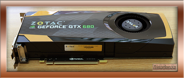

With the release of the GTX 680, Nvidia had indeed gained an advantage in the mission for mono GPU stardom, though its lead was hardly unassailable. AMD’s 7970 boasted 1GB of extra memory and a fatter bus, numbering 384bits upon which to transport it, this, combined with a more attractive price and rapidly evolving drivers, ensured its continued popularity. The 680 however, had party pieces of its own, the first, its own take on AMD’s “powertune” system, whereby the GPU’s speed and voltage is finely optimised in accordance with the card’s maximum power consumption. In the case of the 680, Nvidia guaranteed a minimum speed at which its GPU would operate irrespective of workload, before going on to confidently predict the likelihood of a 5% (or 58mhz) bonus for the majority of the end-user’s requirements.

This brings us nicely onto another notable improvement, the card’s power limit, a mere 195 watts, 55 less than the 7970. Less power proved to be cooler and quieter, attracting numerous users planning a multi-card setup or high performance build in smaller case. The fact that a lower transistor count, a smaller die, inferior memory bandwidth and considerably fewer shader processors did nothing to prevent the 680 from surmounting the competition was not just a testament to its efficient design but also a sign that Nvidia had a copious quota of stops left to pull. What’s that? How many GFlops? What about the texture rate? I told you I’d refer to what was worthy in the context of the narrative, please consult the tables for the rest, its all there, I promise!
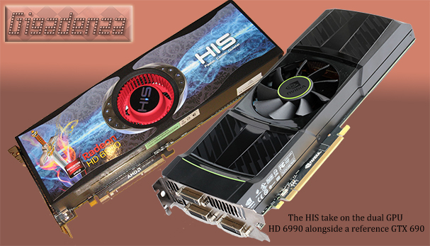
On the Dual GPU front, things were extremely close. The older 40nm process had initially represented something of a disaster for Nvidia. The GF110, or “Fermi” chip was ridiculed for its gluttonous power demands and even though these had been partially curtailed by the time the GTX 580 saw light, the company decided to become more conservative when assembling its dual GPU equivalent, the GTX 590.
The GPUs core speeds were dialed down from 772mhz to just 608, while memory was also restrained by effectively over 0.5ghz. Meanwhile, on the red team, AMD’s own 40nm top dog, the “Cayman”, which had piloted the HD 6970, had proven slower in singles competition but a touch less taxing on the national grid, resulting in a far more bullish approach for the double encore. 7
Indeed, the HD 6990 was the closest we had yet come (save for unofficial efforts by vendors such as Asus) to savouring two fully unencumbered flagship GPU’s sharing the same PCB. Stock core speed was cut by just 50mhz, while the user was invited to take liberties by activating a secondary BIOS via a physical switch on the card’s backplate, which raised the voltage of each GPU and utterly nullified this reduction, albeit at the expense of watts.
