The Case of the Befuddling Base Clock
To expend the bandwidth bestowed by class leading instruments of dynamic random recall should have been a motivating mission. However, as soon as one pondered the compulsory methodology and conceivable ramifications in attending to it, inspiration was abruptly overhauled by apprehension. Remember, the memory controller now shared room and board with the core(s) and any alterations made to the host clock would have a proportional and simultaneous influence upon the speeds of both.
Their statistical correlation was governed by the ratio separating the internal base clock and the memory controller. Depending on the RAM installed and value proposed for processor’s base clock, this ratio would affect an incremental ladder of frequencies for the memory, also known as “dividers”. For mainstream adopters of Sandy and Ivy Bridge based builds, these dividers were a bothersome impedance.
Though the resulting memory frequencies could be manually specified, the actual number available and their proximity to each other, lay at the mercy of Intel’s microcode and the intricacies of the motherboard’s BIOS. There was no certainty of a step on the ladder that would enable both the processor and memory to be close enough to their target frequencies to ensure stable or swifter operation.
Moreover, for the standard 100mhz host clock, even when factoring in its meagre flexibility, DRAM frequencies exceeding approximately 2666mhz were strictly out of bounds since memory frequencies climbed in steps of 266mhz and the steepest supported base clock to memory ratio was 1:10. (10X266 = 2666)
To partially assist, yet another strap situated between the base clock and memory ratio was introduced on the Ivy Bridge platform.
This strap, which for the sake of succinctness we’ll call the “memory strap”, imposed a ratio of either 1:1 or 1:33 relative to the CPU’s Base Clock. Thus, 1mhz for the base clock could represent 1 or 1.33mhz for the RAM and 100mhz translated to either the same, or 133mhz. In contrast to the Base Clock’s straps, neither memory strap offered any margin for fine tuning but its marriage to the existing memory ratios (or multiplier), meant that tweakers could now access two sets of frequencies (or dividers), one ascending in increments of 266mhz as before and the other in shallower steps of 200mhz. All of which made the puzzle of coaxing elite class DIMMS to comply with their prescribed and heavily publicised XMPs decidedly less daunting, and more likely to be solved at no cost to stability.
The Haswell and Hawell-E along with their accompanying chip sets, elegantly blended the bouncing base clock with the memory strap the to complement their investors with an exponentially augmented abundance of steps, straps, ratios, dividers and frequencies . Yes? And? How precisely does that cure our plight? A written response would involve too many figures to coherently construct in paragraphs, so let us proceed to absorb information in as pleasurable fashion as printed statistics will permit.

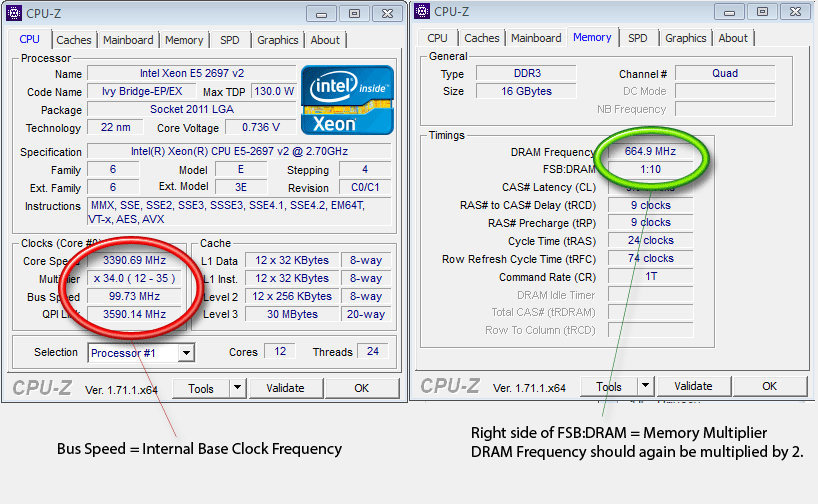
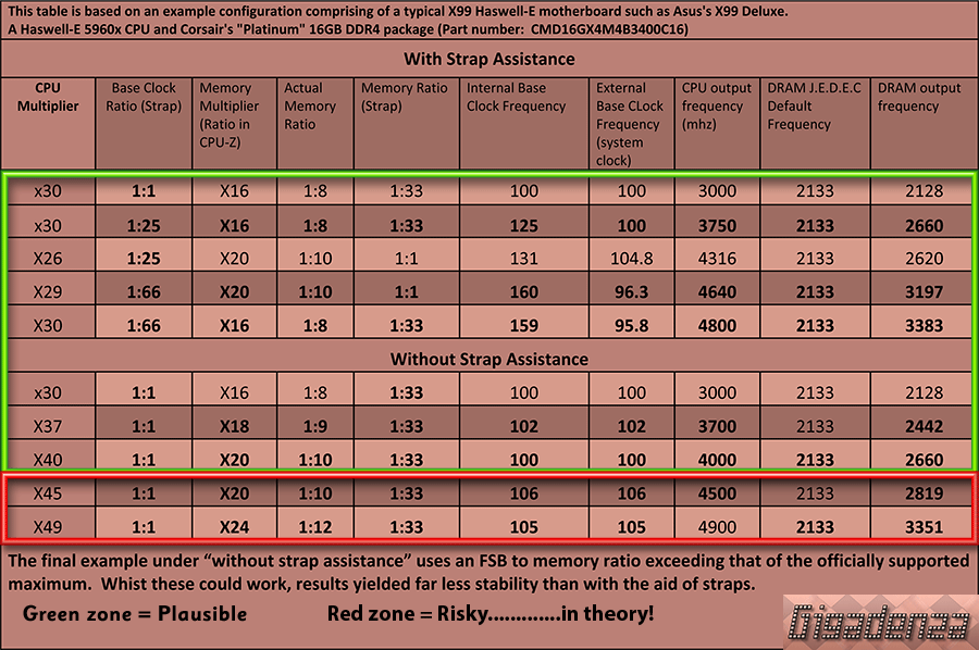
May I humbly present an inspiring, enlightening and indisputably imperative table (coming soon), artistically preceded by a graphical thesaurus (above) and a couple of complementary clipboard snippets (below).

Newly Applicable Formulae
CPU Frequency = Internal Base Clock frequency x CPU multiplier
CPU Frequency = Base Clock Ratio (Strap) x External System Clock Frequency x CPU multiplier (some people did it this way I have no idea which is more accurate or why and I’m extremely angry about that).
External System Clock Frequency = Internal Base Clock frequency / Base Clock Ratio (Strap)
Memory Frequency (if 1:33 memory strap/ratio used). Either can be used.
A:) 1.33 x Internal Base Clock Frequency x Memory ratio x 2
B:) 1.33 x Internal Base Clock Frequency x Memory Multiplier (as listed in CPU-Z)
C:) Base Clock Ratio x 1.33 x System Clock Frequency x Memory ratio x 2
D:) Base Clock Ratio x 1.33 x System Clock Frequency x Memory Multiplier (as listed in CPU-Z)
Memory Frequency (if 1:1 memory strap/ratio used). Either can be used.
A:) Internal Base Clock Frequency x Memory ratio x 2
B:) Internal Base Clock Frequency x Memory Multiplier (as listed in CPU-Z)
C:) Base Clock Ratio x System Clock Frequency x Memory ratio x 2
D:) Base Clock Ratio x System Clock Frequency x Memory Multiplier (as listed in CPU-Z)
For each group of memory calculations, solutions A and B are the most straightforward, though I was compelled to include C and D due to O.C.D brought on by the discovery of one solitary analysis that happened to favour them. Discount at your discretion. Manufacturers are notoriously inconsistent when it comes to selecting which parameters their BIOSES will incorporate and how they shall be expressed. I can only surmise the tweakers in question elected to rely on the figure their board declared for the systems clock and not multiply it by the base clock ratio, which would have given us the internal base clock frequency. Whatever the reason, the results are identical.

All figures in this table assume an absence of any plausible hindrance and are intended to illustrate the theoretical advantage of additional clock straps. They should not be interpreted as usable or even mildly competent advice!
Furthermore, due to motherboards affording broadly varied granularity, the values disclosed in the memory multiplier column should be considered hypothetical and will not necessarily reflect the choices your BIOS provides.
The uppermost spectrum commencing at a blazing base clock rate of 250mhz, was widely regarded as unenforceable at the instant these letters entered the ether, and two years earlier, it had been Asus who were suspiciously brisk to assert that no processor destined to permeate their laudably lavish laboratories was or would be capable of traversing it, despite their distinctly arrogant claim to have implemented the option through ingenuity they refused to reveal. All of which arouses abundant curiosity as to why?


